|
SSA Adapter 4-D
The 4-D resembles the 4-G on the front as to components and
layout. The backs differ in the layout for J12-13 and the outlines for
a big FPGA and LEDs.
SSA Front
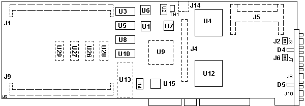
D4 Status
LED Loop B
D5 Status
LED Loop A
J1, J9 Solder
pads for SIMM sockets
J2, J6 Internal SSA ports
J3 "B2" SSA
Loop B Port 2
J4 Solder pads for 140 position
connector
J5 Solder pads for Fast-Write Cache
J7 "B1" SSA
Loop B Port 1
J8 "A2" SSA
Loop A Port 2
J9 "A1" SSA
Loop A Port 1
J14 PS/2 Port (Unknown)
TH1 PTC Resistor |
U1 96H9834
U2 50.0000 Mhz Osc
U3, 5, 8, 10 TC559128AJ-20
U4 Xilinix XC4413-PQ240C 6070
U6 31H8637 BIOS Odd?
U7 Phillips SCC2691AC1A28
U9 Solder pads for 88G6298
U12 34G1521 (Miami module)
U13 Solder pads for Dallas DS1225AD-170
U14 40.000 Mhz Osc
U15 31H8636 BIOS Even?
U29, 27, 26, 28 TC559128AJ-200 |
Simms in J1 and J9
I have both slots filled with 4MB SIMMs, 1Mx36 70nS 5.0v,
PN 82G6981. These have ten chips on one side of the PCB. There are 4 M514400C-70SJ
(data) and one M512200-70SJ (parity) on each half.
J2, J6
The adapter card has 2 internal SSA connectors and 4 external
connectors. This allows one of the 2 dual-port SSA nodes to be connected
either internally or externally to the system unit. The internal connectors
are 2 x 3 pin SSA connectors.
Ports B1 and B2 have both internal and external
connectors. The marking also indicates that ports A1 and A2 are paired,
that is, they are connected to the same SSA loop interface chip.
Similarly, ports B1 and B2 are paired.
+5 V power is available on the connector to power an external optical
extender.
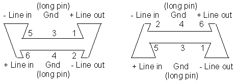
Interior SSA Port Pinouts
Thanks to David Ress for finding this after I lost the
reference... Pin 1 is marked on the outside of the header on the PCB.

1 Line Out + 6 Line Out -
2 Ground 5 Ground
3 Line In - 4 Line In +
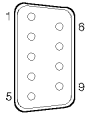
J14 Exploration
Dave Ress tips back his miner's helmet and says:
I checked the SSA adapter I have, and it has the solder
pads for a 6-pin port, but that is all. Looking at the A side and numbering
the solder pads from left to right, I find:
Pad 1 - GND
Pad 2 - Pin 5 of U7
Pad 3 - Pin 4 of U7
Pad 4 - Pin 3 of U7
Pad 5 - Pin 6 of U7
Pad 6 - +5 V
Looking at: SCC2691AC1A28
we learn that U7 is a UART, so the PS/2 port is really a serial port as
the pins of U7 are mapped as:
Pin 3 - RxD
Pin 4 - TxD
Pin 5 - MPO => multi-purpose output (clock pulse?)
Pin 6 - MPI => multi-purpose input (clock pulse?)
Beyond that, I have no idea where the U7 chip interfaces to. I tried
to map D0-7, but no luck there.
SSA Mini-Ports
SSA connectors are 9-pin high-density shielded ITT-Canon
Micro MDSM connectors
 Pin Assignment Pin Assignment
1 Ground
6 Line Out +
2 Line Out -
7 No connection
3 Ground
8 +5 V
4 Line In -
9 Line In +
5 Ground
The serial ports conform to SSA, Level 1. Each port operates at 20MB/sec
full duplex, using point-to-point copper cables up to 25 meters long.
SSA Drive Connectors
David Ress started diddling and said:
I took one of my SSA drives carriers apart this morning. It originally
went into a 7133.
I did this for two reasons: first, I have always wondered how to connect
an internal SSA drive up to the B1 and B2 internal connectors. Second,
if the SSA adapter has just a six pin ribbon connector, I was curious what
the physical connector looked like on the SSA drive.
In looking at the SSA drive carrier, the first thought was "what in
the world?", as the SSA drive carrier has a EURO 72-Pin style connector
(think mini-Nubus). 72 pin connector to support a 6 pin ribbon connector?
But, as it turns out, 32 of the pins are no-connect.
Further disassembling the SSA drive carrier revealed a IBM DFHC 4.5GB
drive, made in 1996. Note: the SSA drive carrier has a label that
says assembled on 23 Feb 2000, I guess IBM had many units left over.
In removing the DFHC I learned that the connector is very unusual, unlike
anything I have seen before. I guess I was hoping to see a SCSI-2 connector
as SSA is a superset of the SCSI-2 protocol, but that was very much wishful
thinking on my part.
SSA Unitized Connector
SSA
Unitized Connector
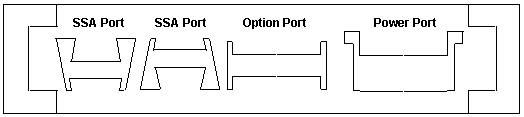
SSA Port on Unitized Connector
Option Port on Unitized Connector
Power Port on Unitized Connector
Carrier connector
4 x 32 female contact, BERG HPC connector, part
number 99F9429.
Fibre-Optic Extender
A fibre-optic extender is available to connect an industry-standard
fiber optic cable within an SSA loop when that loop is used with a 7133
SSA Disk Subsystem. With a fibre-optic extender attached at each node,
the distance between them can be up to 2.4 km. The maximum sustainable
data-transfer rate in a single direction on an SSA link is approximately
18 MB/s. Extending the link with a fiber optic cable results in no degradation
of this data-transfer rate for lengths up to 200 meters, and a gradual
reduction in the achievable data-transfer rate beyond this distance. This
data-transfer rate reduction generally has no effect on SSA subsystem performance
for most applications.
Light Pipes on D4 and D5
Both LEDs are normal LEDs on the PCB. There are light
pipes to transmit the light to the outside.
Each pair of connectors has a green light that indicates the operational
status of its related loop:
| Status of Light |
Meaning |
| Off |
Both SSA connectors are inactive. If disk drives or other SSA adapters
are connected to these connectors, either those disk drives or adapters
are failing, or their SSA links are not active. |
| Solid |
The light is on continuously when power is turned on to the adapter
and both ports for that loop are operational; that is, the devices connected
next to the adapter in the loop have power turned on to them, are connected
correctly to the adapter, and are operational. |
| Slow Flash |
The light flashes continuously if one of the ports is not operational.
That occurs when the cable to that port is not connected correctly or the
device connected next to the adapter in the loop is not operational. |
SSA Back
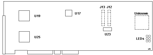
J12, 13 Solder pads for 40 pin
connector
LEDs Solder pads for status LEDs?
U17 VLSI-ARM VY86C06040 |
U19, 25 88H5516
U23 AM29F040-120EC
Unknown Solder pads for big whoppin
FPGA |
40 MHz version of the ARM6 Application-Specific Standard Product
(ASSP) version of the new ARM processor, designed the VY86C06040, is pin-to-pin
compatible with lower clock frequency versions. It operates with
a 40 MHz clock and exhibits a peak performance of 40 MIPS and a sustainable
performance of 26 MIPS at 5
> Dave, are the PCI and MCA variants of the SSA adapter close enough
for the PCI drivers to work? Or do I blame all of this on Jolt slushies?
From my experiences in developing various drivers for MCA
adapters under NT, I will answer "no." This is due to the different
way drivers scan their expansion buses for adapters. PCI drivers scan completely
different from the way MCA drivers do. Some drivers, like the one I am
working on with Ryan A., are written smart enough to scan multiple buses
(in this case, it scans ISA, EISA, MCA, and PCI), but I have found that
to be extremely rare.
9595 Main Page
|