Type 1 Complex
rf90951a
Type 1 Refdisk
rd9095a Diagnostics (common to all
T1-4)
Specifications
Memory
supported, cache, features
256K Cache Daughtercard for Type 1
L2 Cache Performance
ODP vs. ODPR
Support
for >1GB Disks as IML Drive
"G" 486SX 20 MHz
"G" Processor
Upgrade
"J" 486DX 25 MHz 64F0201
"K" 486DX 33 MHz 64F0198
What is the Square
Of Death?
Square of
Death Limits
ECA 0530 OKx complexes
with P/N
Upgrade 486DX2 66/33 92F0145
Supports Non-IML!
Upgrade 486DX 50 MHz 92F0048
"G" 486SX 20 MHz
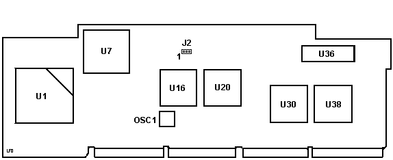
J2 SX / DX
OS1 20.0000 MHz Osc
U1 CPU
U7 57F2194 Memory
Controller
|
U16, 20 78F1659
Memory Data Buffer
U30 78F1659 MCA Buffer
U36 BIOS (AM27C010)
U38 90X8134 DMA Controller0
|
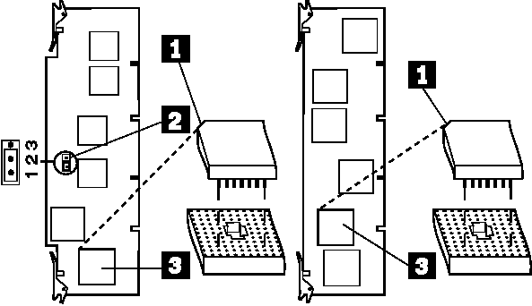
On the 20-MHz board, the jumper 2 must be in positions
1 and 2 if a 487SX processor is installed in connector 3 . If there isn't
a 487SX in connector 3 , the jumper must be in positions 2 and 3.
Optional
Processors for "G" Complexes

© Copyright IBM Corp.
20 and 25 Mhz Processor Boards
For SX models, you can install an optional processor on
a 20 or 25 MHz processor board.
The 25-MHz processor board (above right) has a second processor
connector 3 for either an optional 487SX processor or an 80486SX 25/50
MHz processor. If you install an option processor in connector 3 , of the
25 MHz board, you do not have to remove the existing processor (it is overridden).
Carefully insert the tip of a screwdriver between the
processor and the connector edge and gently twist the screwdriver (around
all edges) until the processor raises up.
NOTE: When you reinstall
the processor, align the beveled corner 1 with the beveled corner marked
on the board.
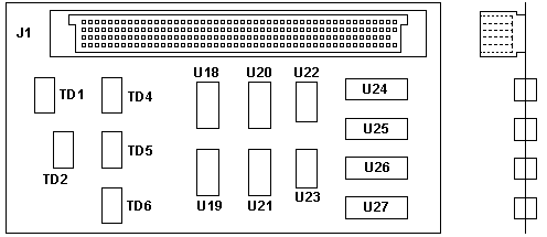
256K 17nS
Cache Daughtercard
Side Toward Complex

J1 159 Pin Header AMP
650754-1
TD1 Fil-Mag 77Z14A030
TD2, TD4 Fil-Mag 77Z14A025
TD5, TD6 Fil-Mag 77Z14A045 |
U18-U21 SDT 74FCT646ASO
U22, U23 TIT031XS AS573A
U24-U27 Toshiba TC55329J-17 |
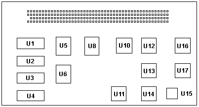
Side Away From Complex

U1-U4 Toshiba TC55329J-17
U5, U6, U8 TI SN74ACT
2160-17FM
U10 AMD 64F6043
U11 AMD 84F8257
U12 AMD 64F6065 |
U13 AMD 84F8261
U14 AMD 64F6046
U15 AMD 64F6048
U16 AMD 84F7970
U17 AMD 64F6066 |
Ed. The chips change from module
to module. Yours may be different.
256 KB Cache Memory Option Kit,
6451095 (64F0199 same thing)
L2 Cache Performance
From Us, the god-Emperor of Microchannel
Praytell, what use can one make of the 256K cache for
the T1 complexes? I hate to admit it, but I never noticed a large (or
significant) boost when I added one.
From Tony Ingenoso
The effects of modern bloatware on a write-through can
be disheartening... IMO IBM's matched cycle scheme goes a long way towards
helping keep the L1 lines filled at a brisk pace even when no L2 is present.
The T2's abnormally good performance (considering its other genetic limitations)
shows this well. For all practical purposes, 90/95's have a 64 bit
memory subsystem working to fill the L1 lines.
From Charles Lasitter
What do you see with one speed processors (DX50) that
are coupled with a faster cache 64F0050, or the T3 and integrated cache?
Since they don't have a 'fall back' processing speed in the event of an
L1 miss, but rather use a 12ns L2 vs 17ns, is there any difference for
them?
I believe we've seen LARGE increases in speed when doing
something like kernel rebuilds compared to no cache. I think it may
depend on what you're doing and the operating system.
From Tony
I don't see this as a core multiplier issue -- even the
low end DX25 T2 runs better than one might expect it to. The kernel rebuild
improvements aren't suprising - compilation algorithms and the bits of
data they work tend to be well localized if modules aren't too massive.
Initial parsing would be very read intensive as well and should make good
use of an L2. Cache perf is indeed a very task specific kind of thing.
Scattered code/data can effectively neutralize it totally.
DX50's are strange -- they often outrun DX2-66 when main
memory bandwidth or I/O is the constraint. When staying in L1, then
the DX2-66 wins due to the multiplier. With a fast L2 and fairly
scattered code/data a DX50 is going to do very well.
From Peter
Uhmmm ... I had the occasion to test a T1 DX2-33/66 board
under Linux. And compare it with the same T1 DX-50 (!) board - both with
the L2 cache.
The 486DX2-33/66 showed 33 BogoMips, the DX50 25 only
... same as the T3 DX50 while a DX2-50/100 (Intel DX4-100 in 2x mode)
on a T3-platform runs at -supposed- 50 Bogomips almost.
In the practical use the T1 DX50 wasn't much slower than
the T1 DX2 - the XF86 stuff paced at the same rate on both. None of the
machines "felt" faster or slower. The DX4 T3 was a bit faster - but not significantly.
All 3 machines had the same XGA-2 card, the same TR 16/4 network adapter,
the same 32MB Parity RAM and the same IBM 400MB HD with the Linux on it.
The T1 platforms had the "plug on" 256K L2 cache (17ns
on the DX2, 12ns on the DX50) and the T3 had its own integrated cache. I
did not write down all the values ... maybe I should repeat that session
again to get some definite, comparable data.
ODP vs. ODPR
The 169 pin is the ODP-version - substitutes a 487SX with
the 486SX still in place. Important on boards with soldered CPU.
The 168 pin is the ODPR-version, where the -R- stands
for "Replace" ... it replaces the 486SX / 486DX respectively and does
not need the "SX-disable" pin therefore.
SCSI drives
>1GB as IML
Type 1 complexes (with the exception of the DX2-66 Upgrade, 92F0145)
need a BIOS 52G9509 to handle IML drives of >1,023MB. (EPROM in drawing)
The upgrade provides the following additional capabilities:
1. Adapter ROM memory more efficiently utilized to minimize
adapter configuration conflicts.
2. BIOS support for fixed disks up to 3.94 gigabytes per device.
3. Supports "Search IML" from any PUN (Physical Unit Number)
or SCSI ID. The system partition is no longer restricted to only SCSI
ID=3D6. Each fixed disk ID will be searched for a valid system
partition.
4. Allows redundant system partitions (IML).
5. Sharing of SCSI devices. An external SCSI device, such
as the 3511, may be shared between two system units.
The following models are affected:
1. Only the following processor boards with an EPROM module
label having the following part numbers may be upgraded:
PROCESSOR FRU P/N MODEL
EPROM P/N
LOC.
20MHZ SX 92F0049 0GX
91F9812
U36
25MHZ DX 64F0201 0JX
84F9154 OR 91F9812 U36
33MHZ DX 64F0198 0KX
84F9154 OR 91F9812 U36
50MHZ DX 92F0048 P3 (UPGD) 91F9812
U44
It was called the "8590/95 Dual Booting Capability EPROM Package"
Type 1 PART
NUMBER 52G9509 (was 52G9750 - try this if other PN is not known)
NOTE: Use the latest refdisk
and diags. See above...
191-052
IBM PS/2 486/25 AND 486/33 PROCESSOR UPGRADE OPTIONS
190-186
IBM PERSONAL SYSTEM/2 486/33 PROCESSOR UPGRADE OPTION
"J" 486DX 25
MHz 64F0201 (old 84F8036)

OS1
25.0000 MHz Osc
OS2 20.0000 MHz Osc
U1 CPU
U7
57F2194 Memory Controller
U8 142 pin PGA socket for
Weitek
U16, 20 78F1659 Memory Data Buffer
|
U16,
20 54F2958 Memory Data Buffer (old)
U19 17nS 256KB L2 cache daughtercard
U30 54F2958 MCA Buffer (old)
U30 78F1659 MCA Buffer
U36 BIOS (AM27C010)
U38 90X8134 DMA Controller
|
The J complex has been seen in three guises:
142 pin socket for Weitek 4167
Solder pads, but no socket SOD)
No solder pads
"K" 486DX 33 MHz
64F0198
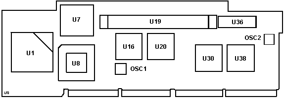
OS1
33.0000 MHz Osc
OS2 20.0000 MHz Osc
U1 CPU
U7 57F2194 Memory
Controller
U8 Space for 142 pin PGA socket
|
U16, 20 78F1659
Memory Data Buffer
U19 17nS 256KB L2 cache daughtercard
U30 78F1659
MCA Buffer
U36 BIOS (AM27C010)
U38 90X8134 DMA Controller
|
Solder pads in U8 are the mark of the SOD.
If your complex doen't have them, it is not affected. Non-SOD complexes
support a Turbochip. (well, usually. IBM made SO many different revisions...)
The K complex has been seen in two guises:
Solder pads, but no socket SOD)
No solder pads
What is the SOD?
> What exactly is this square of death? (SOD)?
It is the mark of the beast. This square of solder pads is actually
the binary equivalent of 666.
David Beem responds:
The missing A1 & A2 pins make this a dead
giveaway for the Weitek 4167. Steven Wachtel reports "memory management"
problems (ECA #0530) with the SOD complex, which might make sense since
the Weitek processors use high memory areas to transfer op codes. So, can
a socket go in place to see if a 4167 would be functional there, or was
it a dropped option? I suppose that with a couple SOD T1s (one of each of
the patches talked about in this thread) & a Weitek 4167 I am one of
those that could answer the question.
>Regarding the sensitivity of this complex, has anyone ever tried
to swap the BIOS with another Type 1 complex that is known to work with
the faster CPUs?
Despite the complexi being very similiar
& using the same reference disk, fundamental changes for things like
the Weitek coprocessor could really mess things up. IBM would issue a whole
complex if there was problems, not just a BIOS change. Other than the
T4 'N' I have seen no
evidence of other complex types checking things like CPUID.
Peter adds:
The only reflection from the past is the comment of an IBM
employee confronted with that exact question. He said "Forget about it".
He then added that the complex had been designed at a time
when IBM was yet "Big Blue" and tended not to give too much control over
their products to one OEM and they therefore integrated provisions for a
"non-Intel" MCU (the Weitek), but the full integration never came.
Practically the SOD can be judged as an analog to the "spare"
dual-in-line artifact solder spots that can be found on many cards, where
the developers planned to build "something" but weren't sure what it could
be and how it should look. Reserve spots in a way suitable for add-ons
or patches, barely attached to the whole board - apart from power, GND
and some basic adress / data / signal lines. The outline matches the Weitek
math-co, but it is (after my knowledge) not supported from neither the glue
logic nor the platform BIOS.
SOD Limitations
from Tim Clarke
The limitation of the 'poor DMA controller' for the Type-1
SOD board appears to be that you can't run a Cyrix/IBM 5x86 at greater that
'x2 clocking' (i.e. 50Mhz in a Type-2, 66Mhz in a Type-1) or an AMD 586
at greater than 'x3 clocking' (i.e. 75Mhz in a Type-2, 100Mhz in a Type-1). Ed. You CAN run a 486DX4-100 ODPR on a SOD.
It's only a 3x multiplier.
Not having a SOD Type-2 I can't test this, but I would
expect the same limits to apply. So, you should be able to run a DX2-50,
DX2-ODPR (@ 50Mhz), Cyrix/IBM 5x86 (@50Mhz) or AMD 586 (@ 75Mhz) in a SOD
Type-2. The 'performance' of a Cyrix/IBM 5x86 @ 'x2 clocking' and the AMD
586 @ 'x3 clocking' are *roughly* equal, although I have a preference for
the Cyrix/IBM chip.
ECA #0530 90-OK9/95-OKD
with Complex P/N 84F9356
Steven Wachtel wrote:
These systems appear to have a memory management problem.
In my environment it was seen on a Model 90 with 16 MB of RAM. The
system would hang during OS2 boot or during invocation of simple processes
after a basic install (such as the system editor ). Symptoms at other
OS2 sites would include excessive "random" trap errors. Not
using DOS on these systems, I would expect the problem to surface as
some indeterminate memory related failure in the E/XMS region.
During initial setup of this machine, the problem
appeared as an inability to create a useable backup reference disk ( if
said disk was used there were always errors ). On restart after the
failure the machine will request to exec its own auto-reconfiguration and
mark out the "bad" regions. For my situation I had the IBM CE on-site
for ~6 days for two separate events. The CE changed each memory chip
and riser (for the M90) multiple times and recombined them in every combinatorial
representation.
Today (11/5/91) after following his instincts and direction
of the higher level support reps, he contacted them again. They asked for
the part number of the CPU board, upon which rests a Gate Array based custom
memory controller. He was advised that there are *known* problems
with the down-rev boards in my new machines. This problem exists(ed?)
on the 0KD models of the M90 and M95, and possibly (as I do not have any
to verify this ) the 0JD models. IBM's second level support is apparently
aware of this potential problem, but has not disseminated this to the CE
level or the purchasing customer.
Problem part identification and rectification:
If the Processor Complex ( nee-CPU board ) part number
is 84F9356 ( or 84F anything ? ) on the "barcode/label" of the board you
should get a replacement.
The replacement part bears the part number 92F.....
I do not know if this is free. Note, I have a M95 with this later
board version that has never hown any of these problems.
Upgrade
486DX2-66 92F0145
192-178
IBM PS/2 486DX2-66 PROCESSOR UPGRADE OPTION
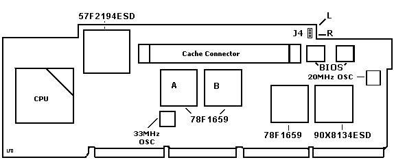
OS1
33.0000 MHz Osc
OS2 20.0000 MHz Osc
U1 CPU
U7 57F2194 Memory
Controller
U8 space for 142 pin PGA socket
|
U16, 20 78F1659
Memory Data Buffer
U19 17nS 256KB L2 cache daughtercard
U30 78F1659
MCA Buffer
U36 ???
U38 90X8134 DMA Controller
|
J4- Once you toggle this jumper
you will end up in a 0129 3000 error - "EEprom Jumper is in the wrong position"
and no boot or such. I'd reported that some time ago while testing around
with the 92F0145.
Most likely it was originally intended to give the -0145 with
2 banks of EEprom to choose between - but by what reason they installed
only one bank and the alternative setting branches into a BIOS error-code
instead.
Peter sez:
As a follow up notice: Yes - it *has* a flash-BIOS. And
- Yes - it comes up with the Type-1 reference disk. Even installs a reference
partition as usual with these disks.
But the system permanently fails to boot into this Type
1 reference partition. Once you reboot it and press [ctrl]+[alt]+[ins]
at CP 66 (cursor top / right) the machine loads the operating system instead
jumping into reference.
The platform nicely takes the Kingston Turbochip *without*
restoration of the system partition. Runs fine with it - right from the
start.
Supports
Non-IML Configurations
Dennis Smith found out that this complex can successfully boot
without an IML device at ID6. He booted a SCSI drive at ID0 WITH NO IML
track. I did it here with my upgrade DX2-66.
His guess was this complex was designed to support RAID
Arrays, and the early RAID controller, "Passplay" had no ability to boot
from an array.
Upgrade
486DX 50 MHz 92F0048
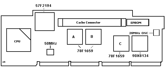
OS1
55.0000 MHz Osc
OS2 20.0000 MHz Osc
U1 CPU
U7 57F2194 Memory
Controller
U8 Solder pads for 142 pin PGA socket
|
U16, 20 78F1659
Memory Data Buffer
U19 17nS 256KB L2 cache daughtercard
U30 78F1659
MCA Buffer
U36 BIOS (AM27C010)
U38 90X8134 DMA Controller
|
Some observations-
The chipset appears the same as other Type 1s with the addition of
decoding circuitry.
FCC ID- ANOIBM486A50
This uses the standard Type 1 EPROM, 27010 / 27C010
L2 Cache- 92F0050
NOTE: This complex needs
the 15nS cache. The other Type 1 complexes use 17nS memory.
From Peter
As far as I can tell (from the pictures of that complex)
it varies through some different wiring and modified ASICs. The part of
the hardware that deals with the CPU clock generation looks a bit different.
The rest of the card is the "later" Non-SOD Type 1 platform as I have it
here in my trusty old AKD.
It seems as if IBM wanted to offer an upgrade path to
DX-50 *without* the ECC option - for those customers that have a -xKx
machine already and for the Mod. 90 maybe, which does not cope with the
"2 layers" DX-50 Type 3 platform very well.
This board was not offered with any particular Mod. 90
/ 95 right from the start. It has been an option only.
Specifications
Memory, Cache,
Features
Min/Max on system board: 8/64MB
RAM: DRAM (PS/2 72-pin SIMM) Interleaved (Install SIMMs in pairs) 70ns
parity checked
Although 80 and 85 nanosecond (ns) memory Single In-Line
Memory Modules (SIMMs) are supported, 70ns memory SIMMs provide optimum
memory performance.
ROM: 128kb
Cache: 8kb L1, optional 256kb L2 J and K complexes
* Socket for optional L2 256K write-through memory cache on "J", "K",
and "Upgrade" DX2-66 (256 K write-thru standard with 486DX-50 ).
* No math coprocessor socket on "J", "K", and "Upgrade"
complexes.
* 24 bit DMA; 10-12 MHz. (10-12? One or the other, please)
* Dual path
memory design (Dual Bus Interleave).
* 20 MB per second data transfer support (for MCA bus)
9595
Main Page
|
