Type 4 Complex
Rf90954a.exe Reference disk for Type 4 Complexes
Rd9095a.exe Common Diagnostics for all 859x
/ 959x Systems
"N" 486DX2 66/33 MHz 61G2343
"P" Pentium 60 MHz 52G9362
"Q" Pentium 66 MHz 92F0120
"Y" / Upgrade Pentium 90/60 MHz
06H3739
Memory supported, cache, features
Support for Convenience
Partition on >3.94GB Drives
Synchrostream Chips
BIOS releases
Flash BIOS 05 from BIOS 03
or less
BIOS Level Revison Features
FDIV Replacement
Diagnostic LEDs
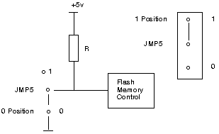
Flash ROM Bank (JMP5)
Serial Link (J5)
Serial Data Link (J3)
"Bad" Memory Reported in Same Positions
Memory
System supports 2, 4, and 8MB parity SIMMs for a max of
64MB.
System supports 2, 4, 8, 16 and 32MB ECC SIMMs for a max
of 256MB.
Cache: 8kb L1, 128kb L2 write-through (DX2-66), 256kb
L2 write-through (P60, P66, P90)
* SynchroStreamTM
Not on N complexes!
* 40 MB per second streaming data
transfer.
* Error Checking
and Correcting (ECC) memory controller
* 20 MHz DMA; 32 bit can directly address all memory, supports Subsystem
Control Block.
* Faster bus arbitration (than Base 1) for busmaster performance.
* Enhanced Dual Path
Memory
* Subsystem Control
Block enabled
* Vital Product
Data support.
* Synchronous
Channel Check support
* Data bus parity
support
* A logging facility is provided (for ECC or system errors)..
Support for Convenience
Partition on >3.94GB Drives
I have personally installed a convenience partition on
a 4.5GB drive and then ran system programs from it. This applies to all
Type 4 complexi, from the 486DX2-66 "N" all the way up to the P90 "Y" complex.
Synchrostream
Chips
From Peter
>That means there are four versions/generations?
In a way, yes. The yellow SSD can be found on 25MHz boards
only - or *should* be present on 25MHz systems only (Lacuna and old Server
720 bridge cards probably), generally none of the older versions made it
into wildlife in significant amounts. I have seen one silver capped SSC
on one P90 platform in an early Server 500 we used at IBM training
center for technical training and this "raw SMD" version (looked like a
"yellow" but with transparent acrylic cover) on a 33MHz Lacuna replacement
board I got as a spare from IBM Greenock - in the vain attempt to fix the
OS/2 video problems under 2.1 ...
>Does this also apply to the P90 complex as well?
I don't think so. I guess they can be found on very early
versions only- if ever. I don't think that the "silver capped" version
was intended for general marketing. The chip itself looked a lot like a
lab proto. Usually the "silver capped" chips have the pins undersides in
a sort of PGA arrangement with IBMs' patented ball-contact soldering -
the SSC is a SMD ship with very dense pins along the sides. The IBM ESD
cap there wasn't a can like usually, but more a shield only glued on top
of the ceramic chip carrier. Had the usual engraved lettering with IBM
ESD54 {7-digit P/N} {date of mfg/sequence number}.
The God Emperor speaks:
I got a P90 complex from Ralph Plewe up in Canada and
it had a ceramic SSC. Tested fine with advanced diagnostics. I have also
had a P60 or P66 with a yellow SSC.
BIOS Releases
BIOS revision 10 is for systems with the single serial
/ single parallel port planars and all Model 90s that have been upgraded
to a Type 4 complex ( 486DX/2-66, P60, P66, or P90). Servers with
the dual serial / dual parallel port planars (e.g. 9595A and PC Server
500) with a type 4 processor should continue to use BIOS revision 8; BIOS
revision 9 will provide NO enhancements for these systems.
Flash Bios 10 Resolves an ABIOS
time/date defect for OS/2 ONLY.
Flash BIOS 09 Seems to have an OS/2 bug. Not on PCBBS anymore...
Flash Bios 08
Flash BIOS 05
Flash BIOS 02
Got a 8595-OKD that came with a Type 4 (P60) complex. Every
time I start it up, Win 95 comes up with the 1980 date. I can take the
ref disk and use "Set Time and Date" and it will show the correct day and
month, but the year will be 2799. Is that Y2K complient or what? You can
change the date and exit back to the Main Menu, then go right back in Set
Date and Time and it is back to the "2799" thing. It has revsion 08 bios.
Any ideas?
Level 10 cured the problem. It seems Win 95, at least
SR2, has the same date problem as OS2 when upgrading a 8595 Type 1 or 2
complex to a Type 4 (P60/66).
BIOS 09 Trivia
If BIOS revision 9 is being used in a OS/2 system, the
system date is required to correct manually every time the system is shutdown
and restarted during the year of 1999. It works fine in year 2000 and beyond.
Use the System Setup utility to set the correct date.
Details: A defect in the ABIOS within BIOS 8 and 9 could
cause invalid system date when boot to OS/2; the defect is caused by mis-handling
of Real Time Clock register's information, and it affects only OS/2. Update
to BIOS 10 will fix the problem. Although it's not required, BIOS 10 can
be installed in systems using other supported operating systems beside
OS/2.
Flashing to BIOS
5 and up from 03 or Lower
If you need to flash a complex,
you can use either 08 or 10. You do not need to configure the complex with
a refdisk before flashing it. Boot with the BIOS update disk, flash it,
and when the update is complete, you can use the latest refdisk and diags
disk to configure the system.
Complex BIOS Levels
Peter Wendt mistakenly divulged:
>Peter, whatthehell is each level bios actually supposed to fix?
Ugh ... have some trouble to recall the changes.
The earlier levels (prior to 03) were
designed for the original P60 / P66 and "enhanced 486DX2" Type 4 platforms.
Level 00 / 01 was
the first shipment level but had some trouble with the SCSI adapters (F/W
SCSI-2 and Server 95 Raid), especially under OS/2.
Supports 16MB Memory SIMMs
Level 02 (rel.
02-23-94) was a first "quick & dirty" attempt to fix it - which was
not that successful.
Added support for 32MB ECC SIMMs.
Level 03
(rel. 09-15-94) finally got it, but had other trouble (cannot remember).
OS/2 2.0 required new IBM2SCSI.ADD and DELIVERY.SYS for support of the
Server 95-Raid adapter. Older IBM2SCSI trap the system if used with Level
03 and above (no longer a topic anyways ). This level adds Fast/Wide
SCSI-2 support within the OS/2 drivers.
3.00 Note: requires
Refdisk ver 1.31 and Diags version 2.31+.
Supports the 90MHZ complex, FRU P/N06H3739, for 9595 & 8641 and
CD-ROMs as a bootable device.
Level 04
(rel. 02-28-95) was supposed to fix all Raid-, Time/Date-, FDD and CD-ROM
(boot) problems under OS/2 - but had a major problem with the memory -
was withdrawn and replaced against Level 05 within a month.
Level 05
(called "Version 1.24 Level 05", rel. 03-22-95) had major changes, especially
for OS/2 2.x and required a new, later reference / diags disk version.
Level 05 was the first level to support the Y complex regularly.
(previous levels might display wrong cpu info in diags / setup).
Note: requires Refdisk ver 1.33 / Diags ver 2.32 +.
Supports 4 GB hardfile, Enables the VPD to display the processor
ID and Step level (shows if a Pentium processor with the FDIV fix is installed).
Allows disabling of the error reporting log POST error which is useful
during RIPL under some conditions.
Resolves the following problems:
Bootable CD-ROM attached to the RAID controller, with an additional
non-RAID SCSI adapter installed. diagnostic problems related to the
CD-ROM being attached to the RAID controller. running SCSI fixed disk diagnostics
with the "read verify" option selected.
Level 06
Never seen. Either not issued or superseeded before release.
Level 07
(rel. 10-27-95) ... no idea. Has been an intermediate release May have
contained a "work-around" for the P90 FPU-bug (not sure).
BIOS code was added to support switching a single keyboard and monitor
between multiple systems.
Level 08
(rel. 01-16-96) came to fix "various problems" with the P90 platform and
the IBM Fast / Wide Streaming Raid Adapter /A - which came with the Server
500. Level 08 was mainly intended to be used with the 8641 (Server 500)
only, since the F/W-SR was not generally announced for the 9595A (but works
though - the number of drives however was limited to 3 due to power- and
heat-problems).
The Level 08 might have various sublevels
(avoided to write "subversions" ... some people might get that wrong :-)
), which differ by date of announcement but aren't explained anywhere.
Most likely they fix some typo-errors / different language support.
Level
09 (rel. -funny- 01-16-96 still) now - as it seems - is
the last Level 08 with integrated Y2K rollover fix. Rem.: The (rel. mm-dd-yy)
refers on the date the $000x000.IML files have.
Level
10 Resolves an ABIOS time/date defect for OS/2 ONLY. But-.
It seems Win 95, at least SR2, has the same date problem as OS2 when upgrading
a 8595 Type 1 or 2 complex to a Type 4 (P60/66).
Would say that Level 05 was
the first BIOS that really worked. If your machine has a downlevel BIOS
- use at least 05 if you have an IBM Fast/Wide SCSI-2 Adapter /A or the
IBM SCSI adapter with cache /A. If your machine has the Server95-RAID adapter
/A (codename "Passplay" without external port) or the IBM Fast/Wide Streaming
Raid Adapter /A (codename "Cheetah" with external port) you should have
Level 08.
FDIV Processor Replacement
Pentium®
processor Replacement (FDIV) Information
If you have a -xPx or -xQx complex (even the mighty -xPx), chances
are it has the FDIV bug. Intel will swap out your processor with a like
processor. Same speed. No upgrade for the FDIV chip is available. Read
the stuff on this link. It will give you the phone# and the requirements
for swapping the chip out (Includes the CPUID
program to identify the presence of the FDIV bug). You will have to give
them a credit card number.
They will send out a non-FDIV chip and a pre-paid shipping
envelope. You pop the old chip out and return it to Intel. If they do not
receive the old chip within 30 days they will charge the credit card number.
I had my replacement in under a week of my call....
Diagnostic LEDs
(Extrapolated from the Type 3 information)
The Type 4 processor board has two LEDs; one in
position CR1, and one in CR2. CR1 lights momentarily at the start of POST,
then turns off, CR2 stays on during POST, then turns off.. No known list
of codes.
Flash ROM Bank
(J5)
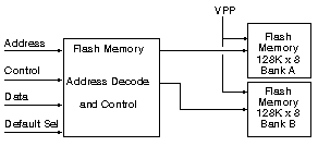
 This jumper on the processor complex is used to select which bank of flash
memory is accessed as ROM. The ROM subsystem consists of 256KB of flash
memory in two banks of 128KB. If the jumper is in position 0 when the system
is powered on, bank A is mapped to addresses hex 000E0000 to 000FFFFF and
hex FFFE0000 to FFFFFFFF. The system is shipped with the jumper in
position 0 (bank A selected).
Note: Don't move jumper while system
is powered-on; unpredictable operation will occur.
 Access to ROM
or RAM at address space hex 000E0000 to 000FFFFF is controlled by the bits
in the memory controller registers. When ROM is enabled, it is not parity
checked. If the jumper is in position 1, bank B is mapped to these addresses. Access to ROM
or RAM at address space hex 000E0000 to 000FFFFF is controlled by the bits
in the memory controller registers. When ROM is enabled, it is not parity
checked. If the jumper is in position 1, bank B is mapped to these addresses.
Peter said:
Originally planned for a sort of "emergency mode". Once
you screwed up the Flash-BIOS you could toggle the bank, insert any working
flash update in the FDD A: and restart the machine, which takes the
flash-image from the floppy drive and recovers (as it can be done on the
704 in the "Bios recovery mode"). However: the base boot-BIOS lacked the
required routines to delete the loused up bank of the Flash-ROM ... and
as far as I know the loading of an image from Floppy does not work.
Another useless feature.
Serial Link (J5)
Serial Link Intended for use with an earlier system management
adapter, which didn't made it to the salesroom. The idea was to supply
a sort of status-link to the processorboard and the SCSI- adapter(s)
and the (possible) backplanes on the later servers.
Aug. 1994
... IBM TECHNICAL DISCLOSURE BULLETIN .
Method to Extend Personal Computer System Memory
July 1994
... IBM TECHNICAL DISCLOSURE BULLETIN
Personal Computer Processor Upgrading
Serial Diagnostics Link
Nov.
1994 ... IBM TECHNICAL DISCLOSURE BULLETIN
Serial Diagnostic Link for PS/2 Model 95 Processor Cards
Disclosed is a Serial Diagnostic Link (SDL) for the PS/2* Model
90 and 95 information panel, allowing the main system processor direct
access to the alphanumeric display. This display is used during Power-On
Self-Test and during error conditions, as information regarding the execution
of the processor is reported to the user. With the SDL, the main processor
does not have to rely on the operational condition of any other system
function to display information on the alphanumeric display.
Without the SDL, the Model 95 information panel
interface can be used by the main processor only when the Micro Channel*,
the planar board VLSI, and the processor complex card interface are the
functional. The SDL is a three-signal interface. Output signals from the
processor card, which are input signals to the information panel used to
program the alphanumeric display, are DISPLAY_STROBE, and DISPLAY_RESET.
The DISPLAY_SENSE signal is an input to the
processor card from the information panel, which is the logical NOT
of the DISPLAY_STROBE. The DISPLAY_SENSE signal is used by the processor
to determine the presence of the SDL and to provide a real-time mechanism
for monitoring the SDL itself. The interface is operated in a uni-directional
mode, with all information emanating from the processor card.
Fig. 1 is a schematic diagram showing the address/write contol
logic and the read back latch used to provide this function.
Fig. 2 is a schematic diagram showing the data deserializer
used to provide this function.
The support hardware on the processor card and on the information
panel for this function is minimal. On the processor card, this logic provides
two bits in an I/O WRITE port, corresponding to the DISPLAY_STROBE and
DISPLAY_RESET signals, and one bit in an I/O READ port, corresponding to
the DISPLAY_SENSE signal. The operation of these signals by the processor
is done entirely with software. On the display panel, logic transforms
the incoming SDL bit stream into the existing parallel interrace to remain
compatible with the alphanumeric display.
Fig. 3 is a timing chart showing the timing of each signal
to display a character on the alphanumeric display. The duration of signal
levels for this interface are defined only by minimums. Since these minimums
are less than the times available in processor card bus cycles, in effect
these signals are timing-independent. No clocking mechanisms are required
for this interface. While the timing of the signals is thus independent,
the sequence of their operation is not.
As shown in Fig. 2, five stages must be performed in the
following order---initial, count/latch, validate/reset, write character,
and validate/hold. The initial stage is entered on a high-to-low transition
of the DISPLAY_RESET signal. The state of DISPLAY_STROBE is a "don't care"
condition when entering this stage. Upon entering this stage, all logic
on the information panel and processor card is reset, awaiting the transmission
of the output character information. The count/latch stage is entered when
the processor produces a high-to-low transition of the DISPLAY_STROBE signal.
In this stage, every high-to-low transition is considered a "count," and
every low-to-high transition is considered a "latch." The logic on the
information panel sequences the "counts" through a 74F393 ripple counter,
the outputs of which are defined as the parallel interface signals necessary
to operate the alphanumeric display. In this way, a simple serial to parallel
interface conversion is performed by the ripple counter. The "latch" is
used to latch the previous parallel output of the ripple counter into a
74F373 register, so that the ripple counter may be reset in the next stage
without destroying the "count" data.
The write character stage is entered on a high-to-low
transition of DISPLAY_STROBE while DISPLAY_RESET is high. Upon entering
this stage, the data is written to the display, and a character appears
at the correct address location. The validate/hold stage is entered on
the
low-to-high transition of the DISPLAY_STROBE signal while DISPLAY_RESET
is high. Upon entering this stage, the data is written to the display,
and a character appears at the correct address location. The initial stage
is re-entered from the validate/hold stage by the high-to-low transition
of the DISPLAY_RESET signal. At this point, the SDL and information panel
are ready for the next output character.
Programming, by the system code, for the stages described
above is straightforward. The following pseudo code shows the general flow
of the stages, with character data values necessary to display ASCII characters
at each address location of the alphanumeric display:
Ed. Not cleaned up, see link to original
article!
OUT DISPLAY_STROBE,1 ; Power on
reset
OUT DISPLAY_RESET,1 ; These
three statements are done at first power
OUT DISPLAY_RESET,0 ; on
to get into the initial stage
TOP:
Move CX, Character
; place the data to be displayed in a
Begin:
; decrement register. Enter Count/Latch
; stage first time thru loop.
OUT DISPLAY_STROBE,0 ; Provide
a "count"
OUT DISPLAY_STROBE,1 ; Provide
a "latch"
LOOP Begin
; Decrement the data, loop until done.
OUT DISPLAY_RESET,1 ; Enter
validate/reset stage
OUT DISPLAY_STROBE,0 ; Enter write
character stage
OUT DISPLAY_STROBE,1 ; Enter validate/hold
stage
OUT DISPLAY_RESET,O ; Enter
initial stage
; Go to TOP to output the next character.
"Bad" Memory
Reported in Same Slots
David Dietz said-
Recently put a T4 P66 complex in my previously functional
8595. Used to
have 64M of RAM using 8 8M 70ns parity SIMMs.
After using the T4 refdisk to get it to recognize the
new complex it said
there was a memory error. Ran the long test and it said I had
bad memory in
B3 and B4. Swapped new memory into B3-B4, Ended up with another
memory error and tested again. Said I had bad memory in B3 again.
Took out A3 and B3 (didn't have any more to put in). Evrything started
working again. put 2 4M SIMMs in A3 abd B3 and 2M SIMMs in A4 and
B4. System came up with 44M.
Booted fine a couple times and then came up with a memory
error again. Ran long test and came up with bad memory in B3 and
B4 again. I'm beginning to wonder if my new complex is burning out
memory in B3 and B4.
Any clues as to what is happening and what I should do
to fix it?
Peter has a flashback and says-
Sounds odd - but ... replace the CMOS buffer battery.
And toggle the "Clear Power On Password" Jumper once when you do that.
Pull out the battery, wait at least 20 minutes, toggle the jumper, install
the new battery and fire the thing up - reconfigure ... and .... ???
I had exactly the same problem back in the mid-90s when
I upgraded an 8595-AKD with a T4 P60 platform. Occasional memory errors
always on the same memory connectors. We'd sprayed them - we swapped and
replaced memory modules (which ran fine in e.g. a 9577 afterwards) - we
did everything you could think of.
Then we replaced the CMOS battery (that CR-2032 3V lithium
cell) ... and the error disappeared. Unexplainable otherwise and not logical.
9595 Main
Page
|
 This jumper on the processor complex is used to select which bank of flash
memory is accessed as ROM. The ROM subsystem consists of 256KB of flash
memory in two banks of 128KB. If the jumper is in position 0 when the system
is powered on, bank A is mapped to addresses hex 000E0000 to 000FFFFF and
hex FFFE0000 to FFFFFFFF. The system is shipped with the jumper in
position 0 (bank A selected).
 Access to ROM
or RAM at address space hex 000E0000 to 000FFFFF is controlled by the bits
in the memory controller registers. When ROM is enabled, it is not parity
checked. If the jumper is in position 1, bank B is mapped to these addresses.